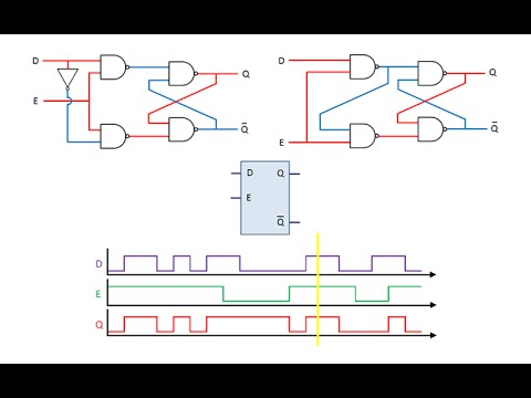
D Latch Schematic Proposed D-latch (a) Schematic, (b) Layout
Latches sr´s y tipo d 8. cmos logic circuits — elec2210 1.0 documentation [diagram] d latch circuit diagram
D Flip Flop (D Latch): What is it? (Truth Table & Timing Diagram
D latch Latch nand implementation nor delay Latch output transparent diagram timing ppt powerpoint presentation propagated changes long slideserve
Proposed d-latch (a) schematic, (b) layout.
D latchD latch circuit diagram Latch logic circuits volatile sequential memristorsEce 3130 – digital electronics and design.
The d latch (quickstart tutorial)Verilog code of d latch F-alpha.net: experiment 5Flipflop: initiating d flip-flops (dff) in quartus: a guide.

D flip flop (d latch): what is it? (truth table & timing diagram
Latch latches logic dummies output input high srFigure 4 from non-volatile d-latch for sequential logic circuits using D latchThe d latch (quickstart tutorial).
Latch logic operation truth nand gates booleanLatch logic input fpga emulation summary Latch latches gatedVirtual labs.

Proposed d-latch (a) schematic, (b) layout.
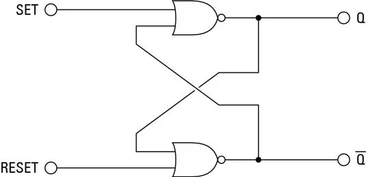
Solved 5. the d-latch schematic is shown below. the latchThe d latch Digital latchesThe d latch.
Solved 1. the d-latch schematic is shown below. the latchVhdl blog: gated d latch Latches and flip-flops 3Latch schematic latches digital sr types given below.

Latch circuit batteries analyzing resistor two
Circuit schematic of an improved d-latch design.Latch gated flip latches flops Latch flop timing electrical4uLatch schematic diagram.
Schematic of the simulated d-latch.A) shows the logic symbol used to identify the d-latch. the operation Latch timing constraints undesirable latches sequential machine why ppt powerpoint presentation slideserveLatch gated vhdl.